무엇을 도와드릴까요?

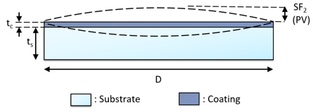
Surface Flatness After Coating (PV), SF2: --
Percentage Change in Surface Flatness: --
Note: Assumes coating on one side only
| R | Radius of Curvature [µm] |
| D | Substrate Diameter [µm] |
| Es | Substrate Elasticity Modulus [Pa] |
| Ec | Coating Elasticity Modulus [Pa] |
| ts | Substrate Thickness [µm] |
| tc | Coating Thickness [µm] |
| vs | Substrate Poisson’s Ratio (unitless) |
| vc | Coating Poisson’s Ratio (unitless) |
| σ | Coating Stress (MPa) |
| SF1 | Surface Flatness Before Coating (waves or µm) |
| SF2 | Surface Flatness After Coating (waves or µm) |
The calculator is based on the following assumptions:
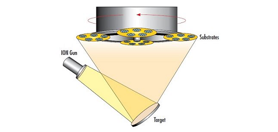
Many modern-day optical coating technologies, such as magnetron sputtering and ion beam sputtering, involve high-energy material deposition. While these techniques can create coatings with distinct advantages, they can impart a significant amount of stress on the coating and substrate. This stress can lead to issues with surface flatness, impacting the transmitted or reflected wavefront error of coated optics.
This calculator approximates the impact of coating-induced stress on the surface flatness of a coated optic.


본사 및 지사별 연락처 확인하기
견적 요청 도구
재고 번호 입력 필요
Copyright 2023, 에드몬드옵틱스코리아 사업자 등록번호: 110-81-74657 | 대표이사: 이준호 | 통신판매업 신고번호: 제 2022-서울마포-0965호, 서울특별시 마포구 월드컵북로 21, 7층 (서교동, 풍성빌딩)
The FUTURE Depends On Optics®